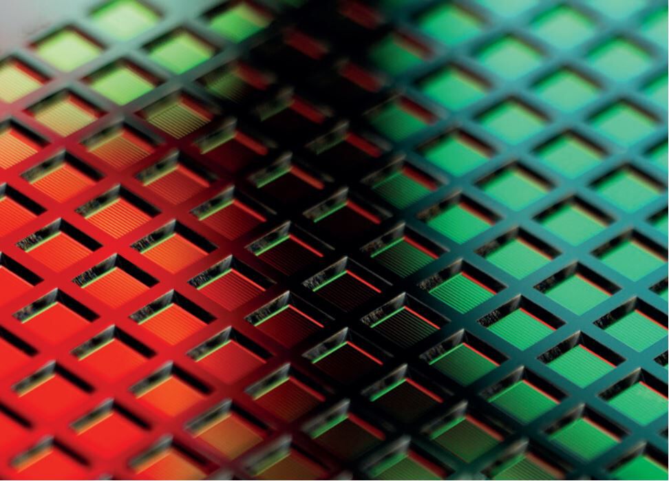
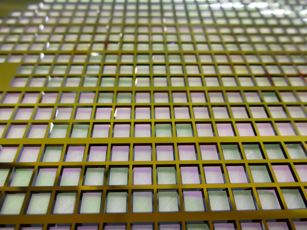
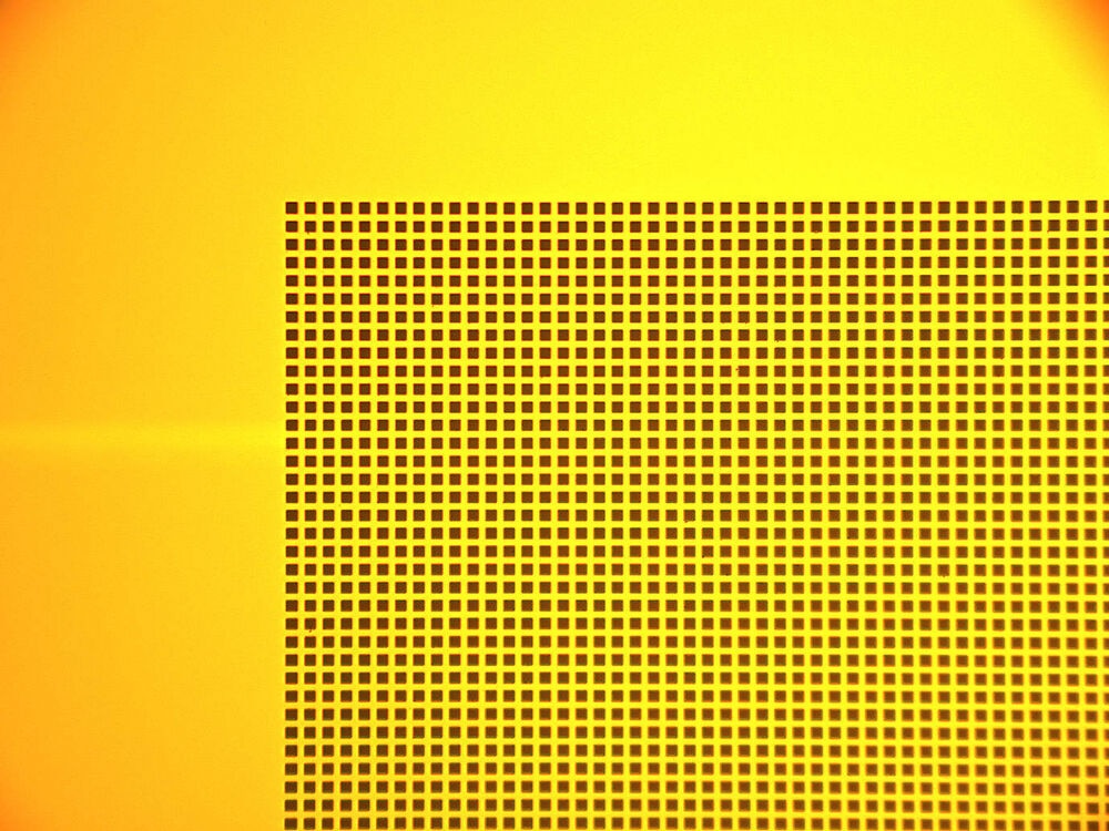
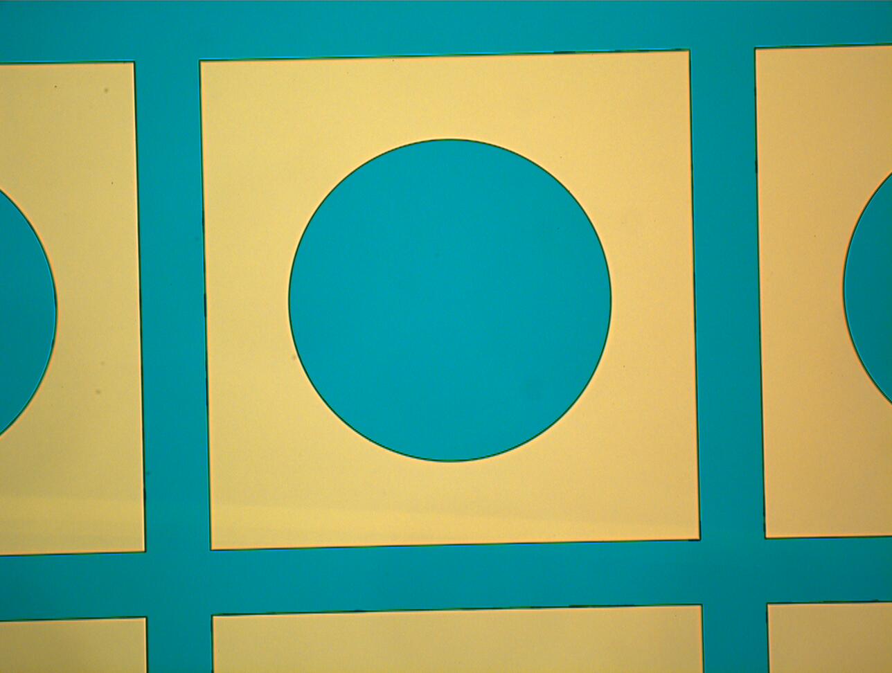
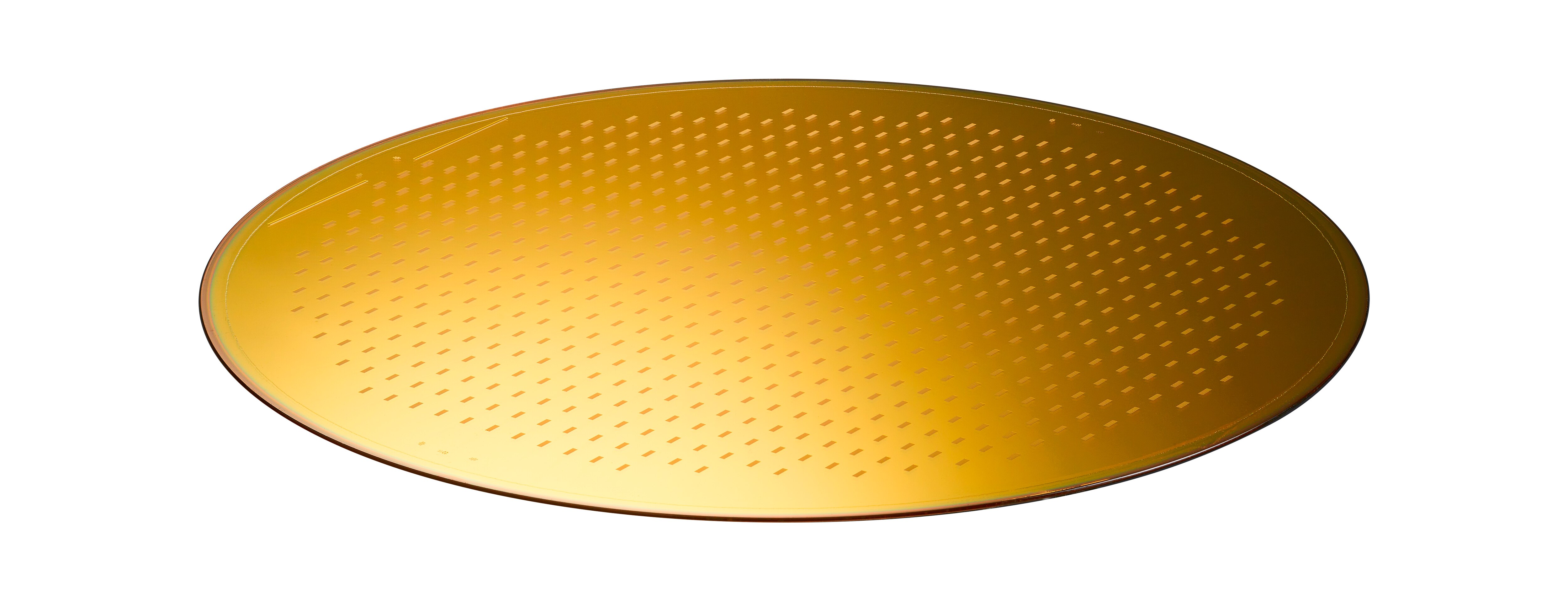
Axetris offers customized micro-structured parts in silicon and fused silica on 150 and 200mm wafers. Mechanical features are obtained by lithography and either dry- or wet-etching. Additional features such as patterned metalizations can be applied, for example as fiducial marks, but also solder frames. The high accuracy and small form factor allows for highly precise components such as submounts or optical benches.
Technical Data
Metric
Imperial
Max. Wafer size
200 mm
Photolithography
Down to 1µm; single/double-sided; thick resists; also on existing topographies
Metallization
Cr, Al, TiW, Ta, Pt, Au, AuSn, others on request
Patterned metallization
As marks, masking, electrodes, solder pads etc.
Dry etching
Silicon, Fused silica, Silicon nitride or oxide, photoresist, others on request
Wet etching
Anistropic Silicon-etching, Glass etching, Metal etching
Dielectric coatings
Silicon nitride, silicon oxide
Membranes
Thin dielectric membranes for sensing, life-science or MEMS applications
Metrology/characterization
Surface measurements; film thickness, resistance and resistivity measurements
Inspection and microscopy
Optical inspection and microscopy; SEM microscopy with EDX element analysis
Dicing
Silicon, glass and fused silica; also with delicate features such as eg. membranes