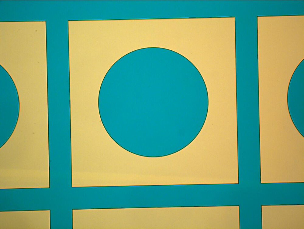
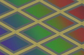
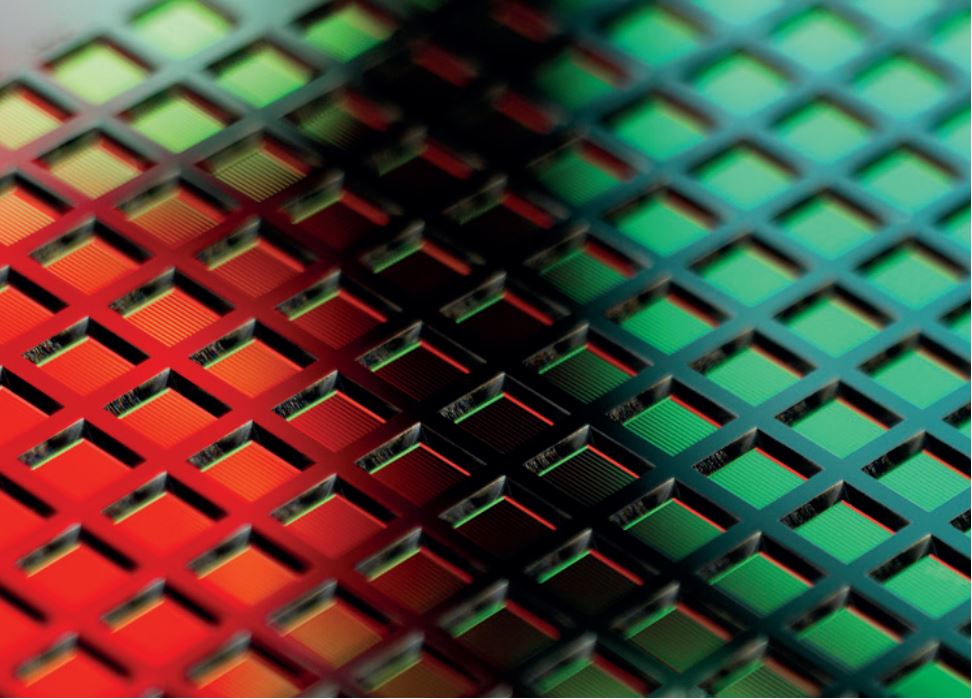
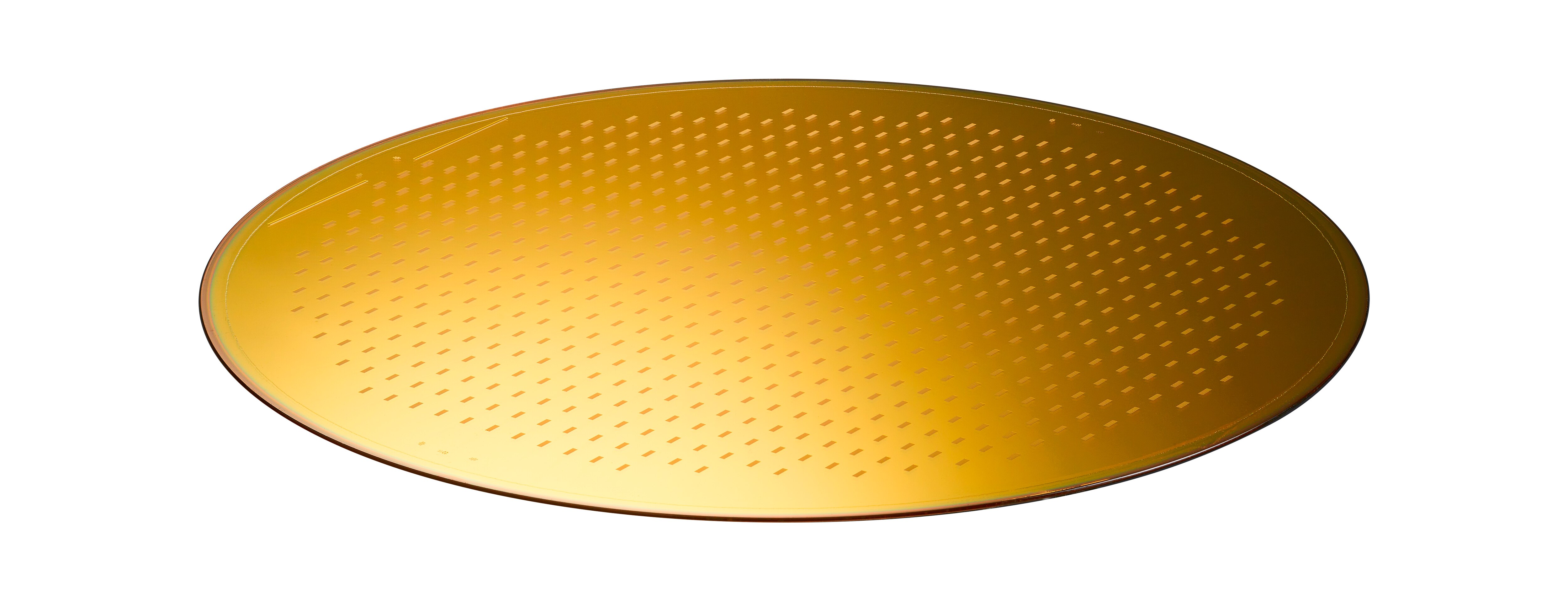
Axetris offers customized patterned metallization on 150 and 200mm wafers. They can be applied to either silicon or fused wafers, or onto supplied and pre-processed customer wafers. The lithographic accuracy and high-quality metal layer depositions are an ideal match for high-accuracy noble-metal electrodes or solder frames (e.g. hermetic packaging). They are delivered as singulated chips or whole wafers, for further processing or wafer-level assembly.
Technical Data
Metric
Imperial
Max. Wafer size
200 mm
Photolithography
Down to 1µm; single/double-sided; thick resists; also on existing topographies
Metallization
Surface measurements; film thickness, resistance and resistivity measurements
Patterned metallization
As marks, masking, electrodes, solder pads etc.
Dry etching
Silicon, Fused silica, Silicon nitride or oxide, photoresist, others on request
Wet etching
Anistropic Silicon-etching, Glass etching, Metal etching
Metrology/characterization
Interferometric and tactile surface measurements, film thickness, resistance and resistivity measurements, optical microscopy, SEM microscopy with EDX element analysis
Inspection and microscopy
Optical inspection and microscopy; SEM microscopy with EDX element analysis
Dicing
Silicon, glass and fused silica; also with delicate features such as eg. membranes